Thick Film Technology
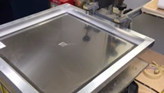
Thick film is used to make electronic devices such as PCB’s and sensors. Using this technology involves the deposition of several successive layers of conductor, resistors and dielectric layers onto an electrically insulating substrate using a screen-printing process. The Thick film process involves many steps that involves a lot of preparation along with a clean work environment.
A product that is using thick film technology is built by screen printing different thick film ink layers onto a base substrate. The base substrate can be a number of different materials: ceramic, stainless steel and in some applications, aluminum.
The thick film inks used to make thick film products are broadly distributed into 3 categories: Dielectrics, Conductors and Resistors. The dielectric materials are generally glass and ceramic based and are not conductive. The conductors contain precious metal particles such as silver, palladium, gold or platinum and their alloys. Resistors are blends of glasses, metals and metal oxides such as silver and ruthenium in various combinations to achieve inks with different resistance values. All the ceramic based thick film inks are blended with glass particles called frit. During the firing process the metal and metal oxide particles bond together in a solid state process called sintering to form a network of millions of electrical connections between the conductive particles. Also during the firing process the glass particles melt, flow and act as an adhesive and filling voids between particles of metal and metal oxides and bonding the entire structure together and to the base substrate.
Vivid Inc. specializes in high-performance coatings, such as thick film technology. Our in-house facility has cutting-edge technology to provide excellent coating applications to numerous industries. Additionally, we ensure to use the latest innovations in the industry to deliver superior results.
We understand that our clients require unique requirements and materials. We complete every job with absolute precision and attention to detail, whether large or small. Beyond just offering coatings, we strive to build long-term relationships with our partners so that they can benefit from our expertise and commitment to quality.
What is Thick Film Technology?
Commonly present in the electronics industry, this coating application is a cost-efficient and dependable solution to create high-quality electronic circuitry and components. It’s widely used to solve the following needs of today’s electronics:
- High communication frequencies
- Miniaturization
- Better circuit density
- Adaptation to new forms (3D and flexible substrates)
- RoHS and REACH compliance
With these features, our thick films address the needs of today’s electronics. It’s constantly evolving to solve future challenges as well. Because of that, it has become a coating technology used in different sectors, such as aerospace, telecommunications, automotive, consumer electronics, medical, and more.
The Main Application of Thick Film
Thick film technology often creates products from three categories: Dielectrics, Resistors, and Conductors. The primary manufacturing process is through screen printing, and ceramic coatings or stainless steel are usually chosen as the base substrate. However, we also use aluminum in some cases.
Some examples of devices made through thick film are as follows:
- PCBs
- Surface mount devices
- Integrated circuits
- Sensors
- Heating elements
The Steps of Thick Film Technology
The whole process involves several steps that must be followed to produce a quality product. Here at Vivid Inc., we strictly follow this process for the best outcomes. Here is an overview of the steps:
Preparation of ink
We prepare ink by mixing the powders (usually ceramics and metals) with a type of solvent or polymer paste. It produces the paste/ink needed for screen printing.
Screen printing
To create the screen printing, the ink or paste is transformed through the patterned woven mesh screen or stencil. Usually, a squeegee is used in this process.
Drying/curing
After the ink has settled after the printing process, it’s dried or cured at a moderate temperature. It evaporates the liquid part of the ink. After that, drying fixes the layer for easy handling or storage before the subsequent processes.
Firing
Therm, glass, or ceramic inks require a high fire temperature. It ensures the layers are fixed permanently in position on the material.
Integration of devices
The final step involves integrating other components to create the finished product or device. Wire bonding or soldering may be used for this stage.
Trust Us to Fulfill Your Thick Film Technology Needs
We understand how each industry requires high-quality and reliable results regarding thick film technology. Here at Vivid Inc., we guarantee superior quality coating services. Our team of experienced professionals has years of experience in this application, and we can deliver results that are second to none.
If you have more questions about our thick film technology process, feel free to contact us today. Our team is ready to answer any concerns, and you can count on us to fulfill all your coating needs. Let Vivid Inc. deliver the quality performance you need!
Materials

- Alumina Ceramic
- Silver


